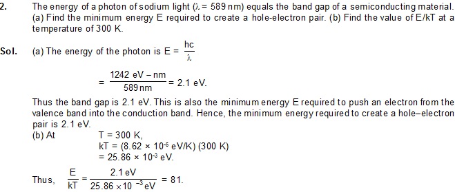
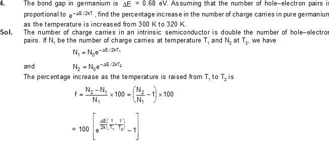
Solved Examples
45.1. The mean free path of conduction electrons in copper is about 4 × 10⁻⁸ m. For a copper block, find the
electric field which can give, on an average, 1eV energy to a conduction electron.
Sol. Let the electric field be E. The force on an electron is eE. As the electron moves through a distance d,
the work done on it is eEd. This is equal to the energy transferred to the electron. As the electron travels
an average distance of 4 × 10⁻⁸ m before a collision, the energy transferred is eE(4 × 10⁻⁸ m). To get 1 eV
energy from the electric field,
eE(4 × 10⁻⁸ m) = 1 eV
or, E = 2.5 × 10 7 V/m.
45.2 Calculate the resistivity of an n-type semiconductor from the following data: density of conduction
electrons = 8 × 1013 cm –3, density of holes = 5 × 10 12 cm –3, mobility of conduction electron
= 2.3 × 104 cm2 /V-s and mobility of holes = 100 cm2/V-s.
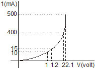
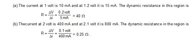
45.3 The i-V characteristic of a p-n junction diode is shown in figure. Find the approximate dynamic
resistance of the p-n junction when (a) a forward bias of 1 volt is applied, (b) a forward bias of 2 volt is applied
45.4 Write the truth table for the logical function Z = (X and Y) or X.
Sol. Z is a function of two variables X and Y. The truth table is constructed in table. The third column gives the
value of W = X and Y. It is 1 when X = Y = 1 and is 0 otherwise. The foruth column of this table gives the
value of Z = W or X.
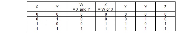
In the first two rows, W = 0 and X = 0. Thus W or X = 0. In the third row, W = 0 and X = 1. The last three
columns of the table collect the values of X, Y and Z which is the required truth table.
The function may also be written as
Z = (X . Y) + X = XY + X.
Questions for Short answer
1. How many 1s energy states are present in one mole of sodium vapour ? Are they all filled in normal conditions ?
How many 3s energy states are present in one mole of sodium vapour ? Are they all filled in normal conditions ?
Sodium vapour ? Are they all filled in normal conditions ?
2. There are energy bands in a solid. Do we have really continuous energy variation in a band or do we have very
closely spaced but still discrete energy levels ?
3. The conduction band of a solid is partially filled at 0 K. Will it be a conductor, a semiconductor or an insulator ?
4. In semiconductors, thermal collisions are responsible for taking a valence electron to the conduction electrons
not go on increasing with time as thermal collisions continuously take place ?
5. When an electron goes from the valence band to the conduction band is silicon, its energy is increased by 1.1 eV.
The average exchanged in a thermal collision is of the order of kT which is only 0.026 eV at room temperature.
How is a thermal collision able to take some of the electrons from the valence band to the conduction band ?
6. What is the resistance of an intrinsic semiconductor at 0 K ?
7. We have valence electrons and conduction electron electrons in a semiconductor. Do we also have ‘valence
holes’ and ‘conduction holes’ ?
8. When a p-type impurity is doped in a semiconductor, a large number of holes are created. This does not make the
semiconductor charged. But when holes diffuse from the p-side to the n-side in a p-n junction, the n-side gets
positively charged. Explain.
9. The drift current in a reverse-biased p-n junction increases in magnitude if the temperature of the junction is increased.
Explain this on the basis of creation of hole-electron paris.
10. An ideal diode should pass a current freely in one direction and should stop it completely in the opposite direction and
should stop it completely in the opposite direction. Which is closer to ideal–vacuum diode or a p-n junction diode ?
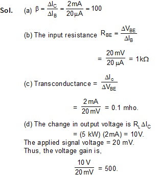
11. Consider an amplifier circuit using a transistor. The output power is several times greater than the input power.
Where does the extra power come from ?
Objective - I
1. Electric conduction in a semiconductor takes place due to
(A) electrons only (B) holes only
(C) both electrons and holes (D) neither electron nor holes
5. A p-type semiconductor is
(A) positively charged (B) negatively charged (C) uncharged
(D) uncharged at 0 K but charged at higher temperatures.
6. When an impurity is doped into an intrinsic semicondustor, the conductivity of the semiconductor
(A) increases (B) decreases (C) remains the same (D) become zero
7. If the two ends of a p-n junction are joined by a wire,
(A) there will not be a steady current in the circuit
(B) there will be a steady current from the n-side to the p-side
(C) there will a steady current from the p-side to the n-side
(D) there may or may not be a current depending upon the resistance of the connecting wire.
8. The drift current in a p-n junction is
(A) from the n-side to the p-side (B) from the p-side to the n-side
(C) from the n-side to the p-side if the junction is forward-baised and in the opposite direction if it is reverse-biased
(D) from the p-side to the n-side if the junction is forward-biased and in the opposite direction if it is reverse-baised
9. The diffusion current in a p-n junction is
(A) from the n-side to the p-side (B) from the p-side to the n-side
(C) from the n-side to the p-side of the junction is forward-biased and in the opposit direction if it is reverse-baised
(D) from the p-side to the n-side if the junction is forward-baised and in the opposite direction if it is reverse-biased
10. Diffusion current in a p-n junction is greater than the drift current in magnitude
(A) if the junction is forward-baised (B) if the junction is reverse-baised
(C) if the junction is unbiaded (D) in no case
11. Two identical p-n junction may be connected in serices with a battery in three ways fig.
The potential difference across the two p-n junctions are equal in
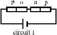
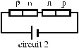

(A) circuit 1 and circuit 2 (B*) circuit 2 and circuit 3
(C) circuit 3 and circuit 1 (D) circuit 1 only
12. Two identical capacitors A and B are charged to the same potential V and are connected in two circuits
at t = 0 as shown in fig. The charges on the capacitor at a time t = CR are, respectively,
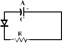
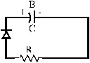
(A) VC, VC (B*) VC/e, VC (C) VC, VC/e (D) VC/e, VC/e
13. A hole diffuses from the p-side to the n-side in a p-n junction. This means that
(A) a bound is broken on the n-side and the electron freed from the bond jumps to the conduction band
(B) a conduction electron on the p-side jumps to a broken bond to conplete it
(C) a bond is broken on the n-side and the electron freed from the bond jumps to a broken bond on the p-side to complete it
(D) a bond is broken on the p-side and the electron freed from the bond jumps to a broken bond on the n-side to complete it.
14. In a transistor,
(A) the emitter has the least concentration of impurity
(B) the collector has the least concentration of impurity
(C) the base has the least concentration of impurity
(D) all the three regions have equal concentrations of impurity.
15. An incomplete sentence about transistor is given below: The emitter-................. junction is........ and
the collector-................... junction is........... The appropriate words for the dotted empty positions are respectively
(A) ‘collector’ and ‘base’ (B) ‘base’ and ‘emitter’
(C) ‘collector and ‘emitter’ (D) ‘base’ and ‘base’
Objective - II
1. In a semiconductor,
(A) there are no free electrons at 0 K (B) there are no free electrons at may temperature
(C) the number of free electrons increases with temperature
(D) the number of free electrons is less than that in a conductor
2. In a p-n junction with open ends,
(A) there is no sustematic motion of charge carries
(B) holes and conductor electrons systematically go from the p-side and from the n-side to the p-side respectively
(C) there is no charge transfer between the two sides
(D) there is a constant electric field near the junction
3. In a p-n junction,
(A) new holes and conduction electrons are produced condtinuously throughout the material
(B) new holes and cinduction electrons are produced continuously throughout the material except in the depletion region
(C) holes and conduction electrons recombine continuously throughout the material.
(D) holes and conduction electrons recombine continuously throughout the material except in the depletion region.
4. The impurity atoms with which pure sillicon may be deped to make it a p-type semiconductor are those of
(A) phosphorus (B) boron (C) antimony (D) aluminium
5. The electrical conductivily of pure germanium can be increased by
(A) increassing the temperature (B) doping acceptor impurities
(C) doping donor impurities (D) irradiating ultraviolet light on it.
6. A semiconducting device is connected in a series circuit with a battery adn a resistance. A current is found to pass
through the circuit. If the polarity of the battery is reversed, the current drops to almost zero. The device may be
(A) an intrinsic semiconductor (B) a p-type semiconductor
(C) an n-type semiconductor (D) a p-n junction
7. A semiconductor is doped with a donor impurity
(A) The hole concentration increases (B) The hole concentration decreases
(C) The electron concentration increases (D) The electron concentration decreases
8. Let E, iC and iB represent the emitter current, the collector current and the base current respectively in a transistor. Then
(A) iC is slightly smaller than iE. (B) iC is slightly greater than iE.
(C) iB is much smaller than iE. (A) iB is much greater than iE.
9. In a normal operation of a tranistor,
(A) the base-emitter junction is forward-biased (B) the base-collector junction is forward-biased
(C) the base-emitter junction is reverse-baised (D) the base-collector junction is reverse-baised
10. An AND gate can be prepared by repetitive use of
(A) NOT gate (B) OR gate (C*) NAND gate (D) NOR gate
Worked Out Examples
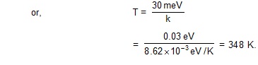
1. A doped semiconductor has impurity levels 30 meV below the conduction band. (a) Is the material n-type or p-type?
(b) In a thermal collision, an amount kT of energy is given to the extra electron loosely bound to the impurity ion
and this electron is just able to jump into the conduction band. Calculate the temperature T.
Sol. (a) The impurity provides impurity levels close to the conduction band and a number of electrons from the
impurity level will populate the conduction band. Thus, the majority carries are electrons and the material is n-type.
(b) According to the question, kT = 30 meV
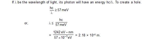
3. A p-type semiconductor has acceptor levels 57 meV above the valence band. Find the maximum wavelength
of light which can create a hole.
Sol. To create a hole, an electron from the valence band should be given sufficient energy to go into one of the
acceptor levels. Since the acceptor levels are 57 meV above the valence band, at least 57 meV is needed to create a hole.
5. The concentration of hole-electron pairs in pure silicon at T = 300 K is 7 × 10¹⁵ per cubic metre. Antimony is
doped into silicon in a proportion of 1 atom in 105 atoms. Assuming that half of the impurity atoms contribute
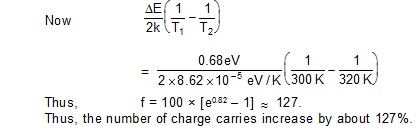
electrons in the conduction bond, calculate the factor by which the number of charge carriers increases due to doping.
The number of silicon atoms per cubic metre is 5 × 1028.
Sol. The number of charge carries before doping is equal to the number of holes plus the number of conduction electrons.
Thus, the number of charge carries per cubic metre before doping
= 2 × 7 × 1015 = 14 × 1015.
Since antimony is doped in a proportion of in 107, the number of antimony atoms per cubic metre is 10-7 × 5 × 1028
= 5 × 10²¹. As half of these atoms contribute electrons produced is 2.5 × 10²¹ per cubic metre. Thus, the number
of charge carries per cubic metre after the doping is
2.5 × 10²¹ + 14 × 1015
= 2.5 × 10²¹.
The factor by which the number of charge carries is increased
In fact, as the n-type impurity is doped, the number of holes will decrease. This is because the product of the concentrations
of holes and conduction electrons remains almost the same. However, this does not affect our result as the number of holes
is anyway too small as compared to the number of condition electrons.
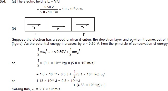
6. A potential barrier of 0.50 V exists across a p-n junction.
(a) If the depletion region is 5.0 × 10⁻⁷ m wide, what is the intensity of the electric field in this region ?
(b) An electron with speed 5.0 × 10⁵ m/s approaches the p-n junction from the n-side. With what speed will it enter the p-side ?
7. The reverse-biased current of a particular p-n junction diode increase when it is exposed to light of wavelength less than or
equal to 600 nm. Assume that the increase in carrier concentration takes place due to the creation of new hole-electron pairs by the light.
Find the band gap.
Sol. The reverse-biased current is caused is caused mainly due to the drift current. The drift current in a p-n junction is caused by the,
formation of new hole-electron pairs and their subsequent motions in the depletion layer. When the junction is exposed to light,
it may absorb energy greater than (or equal to) the band gap. Hence the band gap is equal to the energy of a photon of 600 nm light which is
![]()
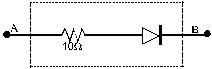
8. A 2 V battery may be connected across the points A and B as shown in figure. Assume that the resistance of each diode is zero in
forward bias and infinity in reverse bias. Find the current supplied by the battery if the positive terminal of the battery is connected to
(a) the point A (b) the point B.
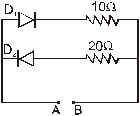
Sol. (a) When the positive terminal of the battery is connected to the point A, the diode D1 is forward-biased and D2 is reverse-biased.
The resistance of the diode D1 is zero, and it can be replaced by a resistanceless wire. Similarly, the resistance of the diode D2 is
infinity, and it can be replaced by a broken wire. The equivalent circuit is shown in figure. The current supplied by the battery is
2 V/10 W = 0.2 A.
(b) When the positive terminal of the battery is connected to the point B, the diode D2 is forward-biased and D1 is reverse biased.
The equivalent circuit is shown in figure. The through the battery is 2 V/20 W = 0.1 A.
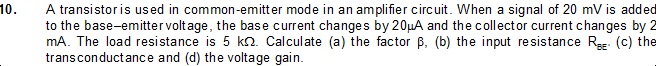
9. A charge of 8.0 mA in the emitter current brings a change of 7.9 mA in the collector current. How much change in the base
current is required to have the same change 7.9 mA in the collector current ? Find
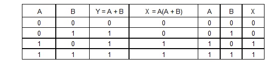
11. Construct the truth table for the function X of A and B represented by figure
![]()
Sol. Here an AND gate and an OR gate are used. Let the output of the OR gate be Y. Clearly, Y = A + B. The AND gate
receives A and A + B as input. The output of this gate is X. So X = A(A + B). The following table evaluates X for
all combinations of A and B. The last three columns give the truth table.
Exercise
1. Calculate the number of states per cubid metre of sodium in 3s band. The density of sodium is 1013 k/g3 How many of them are empty?
Ans: 5.3 × 10 28 , 2.65 × 10 28
2. In a pure semiconductor the number of conduction electrons is 6 × 10¹⁹ per cubic metre. How many holes are there in a sample of size 1cm × 1 × cm 1 mm ?
Ans: 6 × 10 12
3. Indium antimonide has a band gap of 0.23 eV between the valence and the conduction band Find the temperature at which kT equals the band gap.
Ans: 2670 K
4. The band gap for silicon is 1.1 eV (a) Find the ratio of the band gap to KT for silicon at room temperature 300 K (b) At what temperature does this ratio
become one tenth of value at 300 K ? Silicon will not retain its structure at these high temperature. )
Ans: (a) 43 (b) 3000 K
5. When a semiconducting material is doped with an impurity new acceptor levels are created in
a particular thermal collision a valence electrons receives
an energy equal to 2kT and just reaches one of the acceptor levels. Assuming that the energy of the electrons was at the top edge of the valence
band and that the temperature aT is equal to 300 K Find the energy of the acceptor levels above the valence band
Ans: 50 me V
6. The band gap between the valence and the conductions bands in zinc oxide (ZnO ) is 3.2 eV Suppose an electrons in the conduction bands
combines with a hole in the valence band and the excess energy is released in the form of electromagnetic radiation Find the maximum
wavelength that can be emitted in this process.
Ans: 390 nm
7. Suppose the energy liberated in the recombinational of a hole electron pair is converted into electromagnetic radiation if the maximum
wavelength emitted is 820 nm what is the band gaps?
Ans: 1.5 eV
8. Find the maximum wavelength of electromagnetic radiation which can create a hole electron pair in
germanium the band gap in germanium is 0.65 eV.
Ans: 1.9 × 10 – 6 m
9. In a photodiode the conductivity increases when the material is exposed to light it is found that the conductivity changes only if the
wavelength is less than 620 nm What is the band gap?
Ans: 2.0 eV
12. Estimate the proportion of bron impurity which will increase the conductivity of a pure sillical sample by a factor of 100 Assume that each
born atom creates a hole and the concentration of holes in pure silicon at the same temperature is 7 × 10¹⁵ holes per cubic metre.
Density of silicon is 5 × 1028 atoms per cubic metre.
Ans: 1 in about 3.5 × 10 10
13. The product of the hole concentration and the conduction electron concentration turns out to be independent of the amount of any impurity
doped The concentration of conduction electrons in germanium is 6 × 10¹⁹ per cubic metre when some phosphorus impurity is doped into
a germanium sample the concentration of conduction electrons increases to 2×10²³ per cubic metre .Find the concentration of the holes
in the doped germanium .
Ans: 1.8 × 10 16 per cubic metre
15. A semiconducting material has a band gap of 1 eV Acceptor impurities are doped into it which create acceptor levels 1me
V above the valence Band assume that the transition from one energy level
Ans: 20 to 230 K
16. In a p-n junction, the depletion region is 400 nm wide and an electric field of 5× 10⁵ V/m
exists in it (a) Find the height of the potential barrier
(b) What should be the minimum kinetic energy of a conduction electron which can diffuse from the n-side to the p-side ?
Ans: (a) 0.2 V (b) 0.2 eV
17. The potential barrier existion across an unbiased p-n junctions is 0.2 volt. What minimum kinetic energy a hole should have to
diffuse from the p-side to the n-side if (a) the junction is unbiased (b) the junction is forward biased at 0.1 volt and
(c) the junction is reverse biased at 0.1 volt?
Ans: (a) 0.2 eV (b) 0.1 (c) 0.3 eV
18. In a p-n junction a potential barrier of 250 V exists across the junction A hole with a kinetic energy 300 me V approach the junction
Find the kinetic energy of the hole when it crosses the junction if
the hole approached the junction (a) from the p-side and (b) from the n-side.
Ans: (a) 50 me V (b) 550 me V
19. When a p-n junction is reverse biased the current becomes almost constant at 25µ A when it is forward biased at 200 mV. a current of
75µ A is obtained Find the magnitude of diffusion current when the diode is (a) unbiased. (b) reverse -biased at 200 mV and
(c) forward biased at 200 mV.
Ans: (a) 25 µ A (b) zero (c) 100 µ A
20. The drift current in a p-n junctions is 20.0µ A Estimate the number of electrons crossing a cross section per second in the depletion region.
Ans: 3.1 × 10¹³
21. The current-voltage characteristic of an ideal p-n junction diode is given by i = io (eeV/kT –1)
Where the drift current io equals 10µ A Take the temperature T to be 300 K (a) Find the voltage Vo for which eeV/KT = 100 .One
can neglect the term 1 for voltages dynamic resistance of the diode as a function of V for V > Vo (c) Find the voltage for which the
dynamic resistance is 0.2 ohm.
22. Consider a p-n junction diode having the characteristic i = i o (eVKT – 1) where io = 20µ A The diode is operated at T = 300 K
(a) Find the current through the diode when a voltage of 300 mV is applied across it in forward bias (b) At what voltage does the current’ double ?
Ans: (a) 2A (b) 318 mV
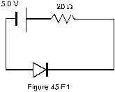
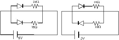
23. Calculate the current through the circuit and the potential difference across the diode shown in figure (45E -1) The drift current for the diode is 20 µ A.
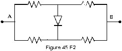
24. Each of the resistance shown in figure (45 E-2) has a value of 20 ohm Find the equivalent resistance between A and B.
Does it depend on whether the point A or B is at higher potential?
In problems 25 to 30 assume that the resistance of each diode is zero in forward bias ans is infinity in reverse bias.
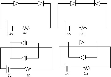
25. Find the current through the resistance in the circuits shown in figure (45 E-3)Ans: (a) 1A (b) zero (c) 1 A (d) 1 A
26. What are the reading of the ammeters A1 and A2 shown in figure (45 E4). Neglect the resistance of the meters.
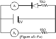
Ans : zero 0.2 A
27. Find the current through the battery in each of the circuits shown in figure (45 E-5)
28. Find the current through the resistance R in figure (45 E-6) if (a) 12 ohm (b) R = 48 W
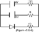
Ans: (a) 0.42 A , 0.13 A
29 Draw the current voltage characteristics for the device shown in figure (45 E-7) between the terminals A and the B.
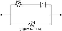
30. Find the equivalent resistance of the network shown in figure (45E-8) between the points A and B